
Transistors, I was once told, "were the fastest acting fuse known to mankind". This of course was a reference to the fact an early transistor was intolerant of fault conditions whereas in years gone by, vacuum tubes (valves) would cop a lot of abuse. Just remember that fact.
Generally transistors fall into the category of bipolar transistor, either the more common NPN transistors or the less common PNP transistor types. There is a further type known as a FET transistor which is an inherently high input impedance transistor with behaviour somewhat comparable to valves. Modern field effect transistors or FET's including JFETS and MOSFETS now have some very rugged transistor devices.
The transistor was developed at Bell Laboratories in 1948. Large scale commercial use didn't come until much later owing to slow development. Transistors used in most early entertainment equipment were the germanium types. When the silicon transistor was developed it took off dramatically. The first advantages of the transistor were relatively low power consumption at low voltage levels which made large scale production of portable entertainment devices feasible. Interestingly the growth of the battery industry has paralleled the growth of the transistor industry. In this context I include integrated circuits which of course are simply a collection of transistors grown on the one silicon substrate.
Transistors work on the principle that certain materials e.g. silicon, can after processing be made to perform as "solid state" devices. Any material is only conductive in proportion to the number of "free" electrons that are available. Silicon crystals for example have very few free electrons. However if "impurities" (different atomic structure - e.g. arsenic) are introduced in a controlled manner then the free electrons or conductivity is increased. By adding other impurities such as gallium, an electron deficiency or hole is created. As with free electrons, the holes also encourage conductivity and the material is called a semi-conductor. Semiconductor material which conducts by free electrons is called n-type material while material which conducts by virtue of electron deficiency is called p-type material.
If we take a piece of the p-type material and connect it to a piece of n-type material and apply voltage as in figure 1 then current will flow. Electrons will be attracted across the junction of the p and n materials. Current flows by means of electrons going one way and holes going in the other direction. If the battery polarity were reversed then current flow would cease.
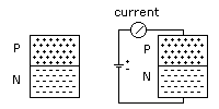
Figure 1. - electron flow in a p-n juction of a diode
Some very interesting points emerge here. As depicted in figure 1 above a junction of p and n types constitutes a rectifier diode. Indeed a transistor can be configured as a diode and often are in certain projects, especially to adjust for thermal variations. Another behaviour which is often a limitation and at other times an asset is the fact that with zero spacing between the p and n junctions we have a relatively high value capacitor.
This type of construction places an upper frequency limit at which the device will operate. This was a severe early limitation on transistors at radio frequencies. Modern techniques have of course overcome these limitations with some bipolar transistors having Ft's beyond 1 Ghz. The capacitance at the junction of a diode is often taken advantage of in the form of varactor diodes. See the tutorial on diodes for further details. The capacitance may be reduced by making the junction area of connection as small as possible. This is called a "point contact".
Now a transistor is merely a "sandwich" of these devices. A PNP transistor is depicted in figure 2 below.
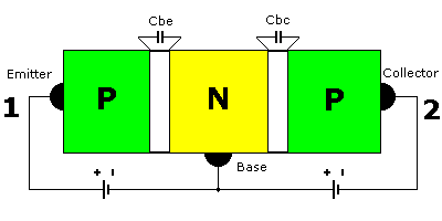
Figure 2. - sandwich construction of a PNP transistor
Actually it would be two p-layers with a "thin" n-layer in between. What we have here are two p-n diodes back to back. If a positive voltage (as depicted) is applied to the emitter, current will flow through the p-n junction with "holes" moving to the right and "electrons moving to the left. Some "holes" moving into the n-layer will be neutralised by combining with the electrons. See electron theory and atoms. Some "holes" will also travel toward the right hand region.
If a negative voltage (as depicted) is applied to the collector of the transistor, then ordinarily no current flows BUT there are now additional holes at the junction to travel toward point 2 and elctrons can travel to point 1, so that a current can flow, even though this section is biased to prevent conduction.
It can be shown that most of the current flows between points 1 and 2. In fact the amplitude (magnitude) of the collector current in a transistor is determined mainly by the emitter current which in turn is determined by current flowing into the base of the transistor. Consider the base to be a bit like a tap or faucet handle.
Because the collector current (where the voltage is relatively high) is pretty much the same as the emitter current and also controlled by the emitter current (where the voltage is usually much lower) it can be shown by ohms law
P = I 2 X R
that amplification occurs. See small signal amplifiers.
We discussed a PNP transistor above. The only differences between PNP and NPN transistors are in manufacturing (i.e. location of the p-layers and n-layers) and of much importance in the biasing. The schematic symbols for PNP and NPN transistors, (the work horse is the NPN) are shown in figure 3 below. A silicon NPN transistor needs to be forward biased by about 0.65V for it to turn on.
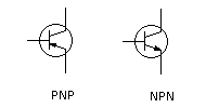
Figure 3. - schematic of PNP transistor and NPN transistor
Notice the only difference is the location and direction of the arrows in the emitter. This denotes direction of current flow in the emitter. Note: that is not a topic I will enter into discussion as I've seen too many discussions already - I have no opinion <G>.
Also see small signal amplifiers.
Download PDF data sheet P2N2222A - plastic bipolar transistor 238K
In figure 4 below I have depicted the schematics of the two most popular types. A J-FET and a dual gate mosfet. Typical types might be MPF-102 for a J-FET and the old RCA 40673 for the dual gate.
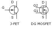
Figure 4. - schematic of J-FET transistor and dual gate mosfet transistor
The FET of course is characterised by its extremely high input impedance. Some people claim the FET is a superior device to a bipolar transistor. I consider that to be a subjective opinion with the proviso that FET development has led to some amazing developments, particularly with power-fets.
I won't go into any length about how FETS operate exceptto point out the principal differences to NPN and PNP transistors. A bipolar transistor has moderate input impedance (depending on configuration) while some FETs can and do have input impedances measured in megohms. Bipolar transistors are essentially "current" amplifiers while FETS could be considered voltage amplifiers.
Download PDF data sheet MPF-102 J-FET 270K
Strictly speaking this tutorial presented by Harris Semiconductor applies more to integrated circuits but the principle remains much the same.
The process of manufacturing semiconductors, or integrated circuits (commonly called ICs, or chips) typically consists of more than a hundred steps, during which hundreds of copies of an integrated circuit are formed on a single wafer.
Generally, the process involves the creation of eight to 20 patterned layers on and into the substrate, ultimately forming the complete integrated circuit. This layering process creates electrically active regions in and on the semiconductor wafer surface.
See - http://rel.semi.harris.com/docs/lexicon/manufacture.html