| Introduction |
Look!
Your life as a lover, as a voter and as an electrical
engineering student, can be changed for the better: if you will read and
try to understand--at least think about--the following.
Warning!
If you don't, you will more than
likely end up behind the bus station, wearing a soiled World War II trench
coat, an unlit stub of a cigar clinched between your rotted out teeth,
a dirty paper bag partially covering your bottle of cheap wine in your
left hand, trying to recall Maxwell's equations while writing them on the
inside of the third stall from the left, in the Trailways rest room. |
|
| As
digital gets faster and faster, it starts to look more like analog than
digital. It is necessary to have a good understanding of the Analog/RF
like properties of fast digital. Attention must be paid to such things
as Transmission Line effects, i.e., impedance matching; parallel and series
termination; microstrip layout; propagation of very high frequencies to
and from the circuit; crosstalk; proper power rail bypass & decoupling;
shielding techniques; as well as groundplane design. |
| One great source of
noise on the power rail--Vcc, is from TTL
(Transistor Transistor Logic) logic. In a typical TTL logic device (gate,
flip flop, counter, register, etc.), it is fair to say that at any one
time: half of the transistors are ON, and the other half are OFF.
TTL is "Saturating Logic," i.e., a transistor is either fully off or
fully on, and in Vsat [1] a saturated transistor requires more
time to become unsaturated than it took to become saturated in the first
place; this time difference is called storage time (Ts).
Therefore, during any logic transition (one/zero or zero/one) All of
the transistors are ON for this short time (Ts)--drawing twice
its normal current. This latency can last from two or three nanoseconds
to as long as fifteen nanoseconds--depending on the logic family.
In systems using thousands, to hundreds of thousands of gates, there
can be a tremendous demand on the power supply, i.e., supplying a constant,
non-varying Vcc (5.0 Volts) to a load that is random and very
high speed (fast di-dt).
If one could supply power to all of the logic devices at a constant
Vcc, everything would be "Peachie Keen." However, Life--and
Murphy, do not allow anything dealing with Engineering Design, to be "Peachie!"
--Bummer!
Because there is "Distance" between any power source and the logic it
powers, a "conductor" or "wire" of finite length is required between this
power source and the logic.
Any "conductor" or "wire" have the properties of resistance and Inductance;
both can cause problems where power is concerned. The resistance problem
can be overcome by increasing the "cross-sectional area" of the conductor.
The Inductive property is likewise amenable to increased crossectional
area, but in a very reduced sense.
Even what might appear to be a small inductance, at high frequencies,
or very high frequencies, can translate to an unacceptable high impedance.
At this point, it is worth noting that TTL logic devices (as with most--spell
that ALL--active devices) have inputs and outputs--you already knew that
didn't you! What you may not have considered is that the power rail--the
Vcc pin--can be both, an input and output "port." You only have to
examine a schematic of such a device to see that the power rail is common
to both input and output stages, i.e., the bias resistors of the input
stage are connected to the same "Rail" as the load resistors of the output
stages.
This arrangement is not a Bad Thing, because it presupposes that this
common power rail "point" will always be held at Zero Ohms! That is, it
will be sourced by an "Ideal Voltage Source."
Together now class: "a Voltage Source--by definition--has Zero Ohms
Output Impedance!
Right?
Right!
Did you get all that Thompkins? Somebody wake up Tompkins[1]--there
in the back...
In the world
of fast edge sensitive logic, it is a simple matter to conceive of "inappropriate
communications" between logic devices (& elements within a device)
through the unprotected, high impedance power rail.
Because of the speed of this demand on the power supply--Rise and Fall
times in the nanoseconds--the frequencies are in the many hundreds of MHz.
And, any conductor, be it printed circuit trace, or wire, any conductor
between the device power pin and the power source can look like an unacceptably
high resistance--tens of Ohms to hundreds of Ohms.
Something as simple as placing a capacitor between Vcc and
Grd. of each logic element--chip, will effectively create this near Ideal
power supply--Zero ohms output impedance!
--------------- TTL (Transistor Transistor Logic) is saturating logic,
i.e., a transistor is either fully off or fully on, and when it is fully
on it is said to be, in Vsat.
It takes longer to turn a transistor off than it takes to turn it on:
the time to turn on (risetime) = Tr the time to turn off = Tf (falltime)
+ Ts (storage time). Ts is the time required for
the hole/electron pairs to move back across the base junction--taking the
transistor out of saturation (Vsat).
[1] Not his/her real name.
|
| TTL (Transistor Transistor Logic) is saturating
logic, i.e., a transistor is either fully off or fully on, and when it
is fully on it is said to be, in Vsat.
It takes longer to turn a transistor off than it takes to turn it on:
the time to turn on (risetime) = Tr
the time to turn off = Tf
(falltime) + Ts (storage
time). Ts is the time required
for the hole/electron pairs to move back across the base junction--taking
the transistor out of saturation (Vsat). |
|
D e c o u p l i n g
|
Decoupling
There are instances where the power distribution between stages cannot
be sufficiency bypassed. In this case, the designer might be tempted to
use several different power supplies. However, by supplying the DC power
to each stage through a separate inductor or "choke," while also bypassing
to ground that stage, the effect is the same. That is to say, the choke
offers a high impedance path to any errant signals or noise between stages,
while offering a very low resistance path to the DC power: this is known
as �decoupling. Active devices such as voltage regulators can also be used
for decoupling stages.
In fact, considering the size of inductors as compared to surface-mount
voltage regulators: regulators might be the better choice. One might better
understand this by recognizing the fact that a choke or inductor is one
of the two needed components for a resonate circuit. Therefore, the combination
of decoupling inductor and bypass capacitor could just happen to resonate
at the wrong frequency. Having said that, it might be obvious that the
inductor needs to be as small a value as is reasonable, and the bypass
capacitor as large as practical. This is essentially correct, however,
there is still the possibility of the resonant frequency of this combination
to cause mischief. And, if that weren't enough, the inductor itself can
be self resonant. This is caused by the distributed capacitance between
windings, i.e., one turn of wire to the adjacent turn of wire, etc...

One more thing to consider about chokes: the "Q" or quality of the
inductor has an effect on its efficiency. As previously stated, the inductor
should appear as a short circuit to the DC power it is carrying, and a
high impedance to any AC, i.e., no series "R." In the practical world this
isn't feasible. However, if heavy current carrying chokes are required,
then the choke must have higher "Q," i.e., less wire which means lower
"R." This can be achieved by using chokes with ferrite cores, which need
considerably less wire for the same value of inductance: it is truly a
multiplier of "Q." Also ferrite beads, i.e., very small donut or tubular
shaped ferrite, are regularly used for circuit isolation, effectively preventing
parasitic oscillations, etc. The down-side of ferrite, is that it will
change inductance as the current or flux changes. In the case of large
currents, it can saturate. However, by correct component choice -- frequency,
AC and DC current, etc. -- ferrite is great tool for the designer. |
| 1... Decoupling is used where the supply voltage cannot
be lowered, i.e., if one needed a noise-free +12 volts on a PC bus, say.
One could get a "clean" +12 volts with a voltage regulator... if only there
was +15 volts or higher to start with. But such is not the case. So you
use a high "Q" inductor (RFC choke) along with the proper bypass capacitor
to effectively lowpass filter the +12 volt supply rail. For a real noisy
supply you can use more than one inductor: a "pie" network for example.
2... One of the most efficient inductors is the ferrite
toroid. It has high "Q" -- low "R" -- and because of its toroidal shape
its fields are confined, and therefore has little stray fields. The super
star of high "Q" inductors or transformers is the pot core. And of course,
don't forget the ferrite bead. Thread the wire through the bead once or
several passes and it may be just what the doctor ordered.
3... Decoupling is only as good as the components that
you use. The capacitor part of the network should be high "Q" and minimum
inductance: the noise is dropped across the inductor, and the capacitor
must exclude the remaining noise. Another way of saying it: in a perfect
world the inductor is an open circuit to noise (AC) and the capacitor is
a dead short -- Zero, Nada, Caput, Zilch; "This here parrot is dead." The
slightest inductance in series with that capacitor, and some very high
frequency noise will come through like Gang Busters!.... Anyway nuff said.
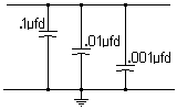
4... SMT or chip capacitors made of ceramic are best.
Also, sometimes in critical circuits, several size caps in parallel are
appropriate, e.g., 1ufd || .1ufd || .001ufd, etc. The reason for this is
as the capacitors become smaller in value, they also get physically smaller,
hence less inductance. However this is less the case with SMT caps: consult
your capacitor data sheets for the impedance verses frequency plots. Didn't
he just say that? |
|
S-h-i-e-l-ding
|
| Shielding can be anything from using a coaxial
or shielded cable, to a sealed conductive chamber for circuit isolation.
Shielding serves a reciprocal purpose: it protects the circuit it is shielding
from outside noise or unwanted signals; and conversely, it contains its
own signals and thus protects the outside world from interference of its
own making. Shielding is mostly used to block electrostatic or "E" fields
(Faraday shield). However, if ferrous metal (tempered Mu Metal works best
for magnetic fields) is used then both electrostatic and some level of
magnetic shielding is accomplished. This is especially useful where open
frame transformers or unshielded coils are used and would otherwise exchange
signals by mutual inductance. |
When is a Shield a Shield?
One important requirement for a shield to be effective, is that there
must be no currents flowing through the shield itself. This is best accomplished
by connecting the reference or common, at only one point on the shield,
thus preventing any flow of current. The reason for this, is that any current
flowing in the shield material itself can produce secondary fields on the
other side of the shielding material and thereby reducing the effectiveness
of the shield. An extreme case of this might be a shielded cable, whose
shield has a different potential at each end, and the resulting current
flow in the shield, inducing unwanted noise into the center or shielded
conductors. (In this situation one might find a remedy by disconnecting
one or the other ends of the cable. However, this may not prove satisfactory
in certain environments, and may require a "Guard" potential, which is
some compromise potential.) |
c i e Shielding
|
| There is an active form of shielding where fields
of counter EMF (equal but opposite) are generated to cancel out the offending
fields. A good and simple example of this is the AC power transformer,
where a "shorted turn" is used to generate a nulling field.
The shorted turn, is a seamless band of copper that wraps the transformer
core in one direction. When cut by the rising and collapsing magnetic flux
-- caused by the transformer action -- the shorted turn acts as a very
low impedance, high current secondary winding, and generates a counter
EMF, and because this winding is shorted, it generates a rising and collapsing
magnetic field of opposite polarity thereby nulling the original stray
magnetic flux. In some cases of severe common mode noise, the shield can
be made to carry an equal but opposite noise current to counter the interfering
noise. However, this is not for the faint-of-heart: any slight change of
the mechanical or electrical parameters, and the cancelling noise becomes
the noise noise!
|
|
G
r o u n d P l a n e
|
| A ground plane is a special and very important component
of any circuit. In essence, it is the return path for all signals including
the power distribution. The ground plane can be thought of as homogeneous
for the DC power only. In all other situations it is strictly inhomogeneous.
All this means that all grounds are not the same. As various circuits use
the ground plane for their signal and power return paths, currents -- conducted
and induced -- are caused to flow throughout the ground plane, and potiently
can affect any or all other circuits, and can cause real problems.
There are only two ways to model the ground plane in a complex signal
environment: and nobody knows what they are!
One can start to understand the function and design (and FM) of ground
planes if one does the following:
1) Draw a map of all signals in a circuit, their inputs, outputs, paths,
and their various connections to and from the ground plane;
2) Then model the inductances, capacitances, parallel and series resistances
while noting the power distribution paths and returns and their respective
noise content;
3) And don't forget all bypassing devices and their contributions to
the model;
4) Since the ground plane is mostly inductive, note must be taken of
any other inductances in proximity to the ground plane, such as transformers,
chokes, tuned circuits, etc., and their contributing fields at all relevant
frequencies.
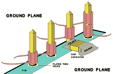
The use of multi-layer printed circuit boards allow the use of multiple
ground planes, as well as buried (under the signal layers) Vcc and Grd.
layers. These layers are sandwiched together and act as a very efficient
distributed bypass capacitor. A variation on this is to have the Vcc and
Grd. layers as the outer or intermediate layers, thus shielding [see foot
note 1] the buried signal layers; or some combination thereof.
|
Input
/ Output
or
"Every Signal Should Have its Own Ground
Return"
|
| When
interconnecting signals--be they analog or digital--to or from any device,
the ideal approach is to have each signal have its own return, or common
path. In the best of all worlds, a balanced (equally referenced above ground)
shielded twisted pair, driven by a high quality differential driver--having
controlled rise and fall times and minium skew--and received by a properly
terminated differential receiver. Being that the world is not always obliging,
a compromise is usually in order: as illustrated by the accompanying figs
in Appendix A.
Common Mode Noise
Common mode noise is any noise that impinges equally on both the circuit
input and its return path, with the same polarity, e.g., both sides of
a differential circuit or twisted pair would have the same sign or polarity,
and in a twisted pair situation with a differential input, there would
be a rejection of all common mode noise.
Differential Mode Noise
Differential mode noise is any noise that is signed such that the input
and the return path have opposite polarities. For example, a differential
input, which would normally reject common mode noise, would be susceptible
to this type of noise.
Video
In the case of interconnecting base-band video signals: the excepted
standard is, and has been, unbalanced 75 ohm coax (RG-59). The nature of
standard RS-170 video is that it covers many many octaves, i.e., ~10Hz
to 4.2MHz; and is a very fragile signal. If one wanted to pick the very
worst transmission medium, it would be hard to pick one worst than 75 ohm
unbalanced coax. The source of the most common and offending interference
or artifact to base-band video, is the ubiquitous 60Hz AC power mains.
This noise manifests itself an a "hum bar" that repeatedly and slowly creeps
up the displayed video. A veritable fortune has been made by many companies
over the years from specialized amplifiers and video processors (proc-amps)
whose sole purpose was to overcome these faults.
If the baseband video standard had been 150 ohm shielded twisted pair,
instead of the 75 ohm coax, the television world would be a much safer
place in which to raise our children.
This problem can be ameliorated by the careful treatment of this coax
in the following ways: first and foremost is to isolate the shield or braid
of the coax. The source of the signal, e.g., the camera, should have its
connector isolated from case ground, and the shield side of the video connector
should be connected directly to the circuit board of the video source.
From here to the destination, the signal common or shield, must never contact
any external ground, common or any other coax's common or shield. Upon
arrival -- whether to a proc-amp, distribution amplifier (DA), ADC, display,
or whatever -- the coax shield must only connect to the signal return of
the appropriate circuit board, and, of course, the coax must be terminated
in its characteristic impedance of 75 ohms.
|
Analog / Digital
One of the hardest things to design successfully, is one having both
analog and digital circuits living on the same board or planer, and sharing
the same power supply. Most designers who have yet to be burned, don't
give it a high priority. In some cases analog and digital on the same real
estate may not be practical, and in other cases it can be down-right hard.
If one is to succeed, it will require that he/she master the above noise
handling Analog/RF concepts.
|
Tips & Suggestions
Ideally one should attempt the following:
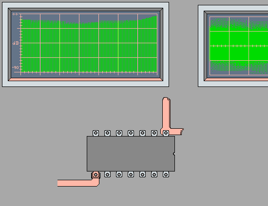
Bypass
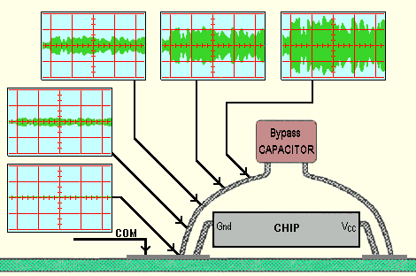
1... .1 ufd or greater, ceramic capacitors (chip surface mount technology,
SMT, preferably).
2... One capacitor per SSI, MSI TTL device.
3... The capacitors should connect Vcc and Grd. of the device, using
the shortest path possible. (See figure)
4... Ceramic chip capacitors have the best high frequency characteristics,
i.e., have least inductance and stay capacitive reactive over a wider
frequency range (offer the lowest impedance).
5... Tantalum will not substitute for ceramic. However, tantalum capacitors
are a good adjunct to the ceramic. That is, they offer low impedance
to the lower frequencies.
6... In some high frequency analog (RF) or high speed digital circuits,
it is appropriate to use several different types of capacitors. Tantalum
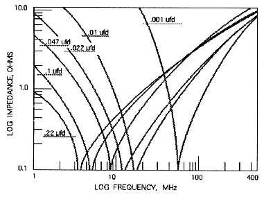
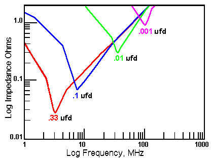
for low frequencies; large ceramic (e.g., 0.1 ufd) for the higher frequencies,
and small ceramic, RF capacitors (~1nfd) for the much higher frequencies.
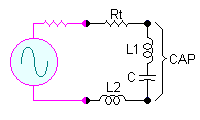
The name of the game is maximum capacitance with minimum inductance.
Remember: when Xc = Xl you have resonance, and that's something you
don't need in a bypass circuit!
|
Decoupling using "L"
1... Decoupling is used where the supply voltage cannot be lowered,
i.e., if one needed a noise-free +12 volts on a PC bus, say. One
could get a "clean" +12 volts with a voltage regulator... if only there
was +15 volts or higher to start with. But such is not the case.
So you use a high "Q" inductor (RFC choke) along with the proper
bypass capacitor to effectively lowpass filter the +12 volt supply rail.
For a real noisy supply you can use more than one inductor: a "pie"
network for example.
2... One of the most efficient inductors is the ferrite toroid. It has
high "Q" -- low "R" -- and because of its toroidal shape its fields
are confined, and therefore has little stray fields. The super star of
high "Q" inductors or transformers is the pot core. And of course,
don't forget the ferrite bead. Thread the wire through the bead once
or several passes and it may be just what the doctor ordered.
3... Decoupling is only as good as the components that you use. The
capacitor part of the network should be high "Q" and minimum inductance:
the noise is dropped across the inductor, and the capacitor must exclude
the remaining noise. Another way of saying it: in a perfect world
the inductor is an open circuit to noise (AC) and the capacitor is
a dead short -- Zero, Nada, Caput, Zilch; "This here parrot is dead." The
slightest inductance in series with that capacitor, and some very
high frequency noise will come through like Gang Busters!.... Anyway
nuff said.
4... SMT or chip capacitors made of ceramic are best. Also, sometimes
in critical circuits, several size caps in parallel are appropriate,
e.g., 1ufd || .1ufd || .001ufd, etc. The reason for this is as the capacitors
become smaller in value, they also get physically smaller, hence
less inductance. However this is less the case with SMT caps: consult
your capacitor data sheets for the impedance verses frequency plots. Didn't
he just say that? |
Signal Distribution
1... "Every dog has its Day," and: Every signal needs its own Ground
Return. Inputs and outputs should be as separate as possible, and
they must not share the same ground return. Think about it: very sensitive
input, very large signal output; a formula for Mister Oscillation.
2.. The layout should follow a flow, like the circuit diagram follows
a flow: there is a "Goezinta" and a "Goezouta."
And, the power supply, and its ground return, should move in
near the output part of the circuit -- where the larger signal levels
(and low sensitivity) live and away from the high sensitivity part of town.
3.. When two, or more, signals share the same ground return, there can
be interference between the two. This is really true for analog,
but digital has some margin before it becomes troublesome. However, this
is not a license to steal: if this happens at more than a few places
and a few times, the cumulative effect can come home to roost in
the form of intermittent trouble, and that my friend will drive you "Nuts,"
and you may never track it down, NEVER!.
Parts Layout
1.. When laying out a board -- PCB or wire wrap -- try to keep all
of the components for that particular part of the circuit together.
Don't think that the timing resistor or timing capacitor for a one-shot
can live on some other part of the board without causing timing jitter
or even false triggering. And remember: Bypass! |
Crosstalk Problem:
1.. Crosstalk can happen when wire wrap wires are bundled. The tighter
the bundle and the longer the wires run together, the worse the crosstalk.
2.. The distributed capacitance between wires is the killer: with the
rise and fall times in the single digit nanosecond range, it doesn't
take much to trigger an edge sensitive device.
3.. In PCB layout the name of the game is to crowd thin traces together
and get data from point "A" to point "B," "C," etc... without using
any board space. If the traces are too close and "stay together" for too
great a distance,it starts to look electrically like a wire bundle,
a tight wire bundle: "A real Bummer Dude!"
Solution:
1.. When wire wrapping, Don't bundle wires, EVER! Use the shortest
wire run from point "A" to point "B." And:
Don't worry what it looks like! In this life you have a choice:
it either looks good and doesn't work worth a Damn, or it looks
like Hell and works great -- it rarely does both. Remember the Hot Rodder's
old saying: "If it won't run, chrome it." Words to live by.
2.. On PCB layout: if a group of signals must run together more than
a two or three inches (more or less depending on the logic family)
across the board: swap sides of the board and/or mix traces so everybody
has new neighbors. |
Power Distribution
1.. Distribution of power to and on a circuit board is fairly straightforward.
In the case of several different power supplies, e.g., +5, +15, -15,
etc., the ground returns are the most important consideration. If there
is a mix of circuit types, Analog, TTL, CMOS, etc., then the analog
grounds must be separate from the digital ground returns. And, sometimes
if there is a large concentration of fast TTL, and some CMOS logic: thought
should be given to separate supplies and, of course, separate ground
returns. The reason for the latter is that TTL, by its very nature,
puts large amounts of noise into its supply rail, and though CMOS is robust,
its merely a matter of degree to what it takes to corrupt it.
2.. There is a school (DUKE) of thought (no, wrong, can't be DUKE) that
says that Vcc leads or runs should be as short as possible. This
is true as far as IR drop (resistance) is concerned, however, up to a point,
the longer the lead, the more inductance, hence the more decoupling.
But, if you buy on to this idea, and its a really good idea,
think about limiting the number of circuits feed by this long wire -- run
more than one "long run."
Summary
Implementing the suggestions in this paper will not be easy, and for-sure
not always possible, but do the best you can and, who knows, your circuit
might work... or NOT. |
Voltage Regulators
Linear Regulators
1.. Read the data sheet. The needes and capabilities of the regulator
are in there somewhere; they might not jump out and bite you right
away, but they are there.
2.. The use of three terminal linear voltage regulators, like
the 78xx and 79xx devices, is fairly straightforward. However, there
are a few things to remember: Always bypass -- there's that
word again! -- the input pin and the common pin with a ceramic capacitor
no smaller than 0.3 ufd, and use absolutely the shortest leads
possible (there are some transistors with pretty high f t in
that regulator, and if you furnish enough reactance of the right
kind, Mr. Oscillation will visit you again).
3.. If your regulator is furnishing power to a capacitive load, and
the primary power is removed -- like unplugging a PC card, or disconnecting
an experimental setup -- the charge in that capacitive load will
cause the secondary or output of the regulator to be more positive than
the primary or input. If this reverse voltage exceeds the regulator's
ratings it will blow up. To prevent this sort of failure, a diode
is placed between the input and output, such that, when
reverse voltages are present, the diode conducts preventing
damage. (see Figure)
4.. There will come a day (or night) when you may need an
eight volt regulator, and all you have is a 7805, five volt
regulator. By inserting a voltage equal to the difference in the
common lead, "Voila," you have 8 volts. You can do this by inserting
a zener diode or a low resistance voltage divider (or a pot for variability).
If all else fails, insert a series of silicon diodes (cathodes toward
Grd.) @ .6 volts per, until you have the desired output.
5.. These regulators don't need an output capacitor per se, but
a minimum of 1 ufd is recommended to prevent fast load pulses from
causing needless error correction by the regulator. As for the primary
or input capacitance, it depends on the ripple content from the primary
voltage: If the voltage is straight from the rectifier, then obviously
large capacitors are required -- assuming a large load on the regulator's
output. The greater the difference between the input voltage and
the output voltage, the less stringent the capacitor requirements.
6... In the data sheet -- you know, that funny looking piece of
paper that causes you to squint, and makes your head feel funny --
In the data sheet, there is information on forward drop, Vfwd, of
the regulator at some current.
This means that if the primary voltage is near the desired secondary
voltage at some current, you may be in "Deep Dudu." The greater the
difference between the input voltage and the output voltage, the
easier life is: if the rating of the regulator is a 1.1 volt drop at 500
ma, and you have a 5 volt margin -- say -- you are in fairly good
shape; if you have, on the other hand, a 10 volt margin, you're in
great shape! |
Constant Current Generator
1... A voltage regulator is, by definition, a "Voltage Source,"
which ideally supplies a constant voltage regardless of the
changing load (within reason). A current source, likewise,
supplies a constant current regardless of the changing load. A
good constant current source, or generator, can be constructed using the
three terminal regulator tied as in the diagram. The VR maintains
a constant voltage (e.g., 7805: 5 volts) across the series sense resistor:
a constant voltage across a constant -- or fixed -- resistance, yields
a constant current. "Gee, that sounds remarkably like Ohm's law." |